By Don Naugler, Harold Hyman & Terry Leahy
Abstract
Surface Mount Rework systems have evolved into sophisticated thermal processing tools with the ability to accurately mimic original reflow oven profiles at a localized rework site. Features such as automated profile generation allow the user to quickly define workable profiles for a wide variety of applications. However, many of today’s applications demand more carefully crafted profiles than can be achieved using traditional methods.
Sensitive components such as optical devices, connectors, and certain package types, to name a few, have specific requirements and limitations that go far beyond the typical solder joint time-temperature profile. Elevated temperatures of lead free processes further amplify thermal management issues.
Rules Based Thermal Profiling allows automated profile generation with a combination of parameters that that are set to meet each situation. Multiple criteria may be specified and prioritized to yield the most reliable process for reworking sensitive components and assemblies.
Introduction
When reworking printed circuit board assemblies (PCBA) the process engineer must develop thermal processes that assure reliable solder joints while protecting delicate components and boards. Ideally, the profile will closely replicate the profile used in the initial assembly process in order to provide the greatest confidence that the assembly will have the same or similar performance and reliability as the original product.
The thermal profile is created to subject the solder joints to a temperature excursion that will cause the fluxing, melting, wetting and cool down operations to occur in a correct fashion. It is generally agreed that, for a given flux/solder combination, this thermal profile should always be the same regardless of the physical make-up of the assembly. However, it is evident that massive assemblies will require a great deal more energy to achieve this “golden” profile than will assemblies of small thermal mass. The secret lies in the ability to generate a thermal cycle that will transfer just the correct amount of heat to the assembly to achieve the desired result.
The thermal management needed to do this has to take into consideration not only the requirements of the solder joints but also the constraints imposed on the process by the presence of the sensitive components that have strict temperature limitations. Once these limitations are known, Rules Based Thermal Profiling can be employed to establish boundaries and to insure they are respected while, at the same time, observing all the requirements for good soldering.
Thermal Process for Rework
Generating thermal profiles for rework is more difficult than generating profiles for reflow in an oven. When an assembly is passed through a reflow oven, the entire mass is heated, resulting in a relatively uniform temperature throughout. Belt speeds and zone temperatures may be adjusted so that the desired thermal profile is achieved.
In the case of rework, heating is localized, for the most part, to the rework site. As a result, profiling is more difficult since thermal characteristics of each component and assembly can vary considerably, one from another.
Heating for rework is accomplished through a combination of bottom side (board heating, or conditioning) and top side (component heating). As the component is heated, thermal energy is dissipated through the board due to its heat sinking effect which is a function of its thermal mass. The mass of the component and the rate of dissipation will affect the required energy and hence the heating parameters.
Bottom heating is used to bring the entire board to an intermediate temperature. This is done to minimize stress caused by local heating, and to reduce the extraction of heat from the rework site. However, since the entire board can not be heated to reflow temperatures there will be lateral temperature gradient, and hence transfer of thermal energy (heat) from the rework site to the surrounding areas.
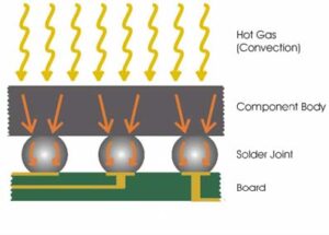
In a convection rework system most of the heating for area array devices (BGA, CSP, Flip Chip, etc.) is accomplished via transfer of energy from the hot gas to the top side of the component. Heat then flows through the body of the component to the component-solder interface, through the solder, through the board-solder interface, and into the board (see Figure 1). Copper conductors within the board, especially large power and ground planes, provide a substantial thermal path to draw heat away from the rework site.
To corroborate this “through the component” heat flow, an experiment was performed to determine the extent of heat transfer due to hot gas flowing under a BGA component. A test board was constructed with a 27mm PBGA mounted on a sample FR4 board. The board was drilled from the back side and a thermocouple was inserted, contacting one solder ball, and secured with thermally conductive epoxy(1).
Two thermal cycles were executed with identical heater parameters (see Figure 2). The rework nozzle was positioned on the board, gasketing to the board surface, and deflecting exhaust air upwards and away from adjacent components. The first set of data was taken using the standard rework process (Cycle 1). Prior to the second cycle (Cycle 2) a thin layer of Kapton tape was placed along the component edges, sealing the gap between the BGA body and the board to prevent possible flow of hot gas under the component body.
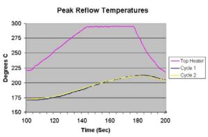
The test showed that taping the gap between the BGA body and the board had no significant impact on the temperature measured at the solder joint, confirming the fact that the majority of heat transfer occurs via conduction through the component body rather than from lateral hot gas flow under the component.
Impact of Materials on Heating
The flow of energy through the component can be damaging if not properly managed. Certain components, depending on packaging materials used and construction, can be especially susceptible to thermal damage due to their low thermal conductivity.
Table 1 provides examples of thermal conductivity for typical materials used in electronic assembly. Ceramic packages conduct heat far better than plastic packages. Polyimide and epoxy based substrates have low thermal conductivities. Thermally enhanced packages, especially those with thermal via connections will conduct heat quite rapidly (but not necessarily uniformly across the package).
Table 1 – Approximate Thermal Conductivity of Various Materials 2,3,4,5
| Material | W/m-°K |
| Copper | 380 |
| Ceramic – Alumina | 29 |
| Silicon | 0.8 |
| Polymide | 0.6 |
| Thermally Enhanced Encapsulant | 0.42 |
| Epoxy Fiberglass (PCB) | 0.26 |
In many cases temperature ramp rates that are acceptable in a reflow oven may not be acceptable in a rework process because of the temperature gradient that occurs between the top of the package (closest to heat source) and the bottom of the package (farthest from the heat source). The process engineer, in considering the choice of ramp rate, should be aware of this interaction between process parameters and needs the ability to take suitable precautions.
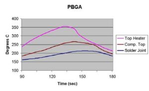
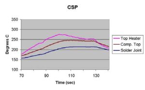
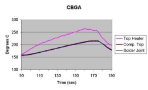
Figures 3, 4 and 5 show peak temperatures from rework reflow profiles generated for three package types. The profiles were created with the main requirement being to provide a peak temperature between 210 and 215º C at the solder joint. The figures illustrate the relative differences in temperature between the top heater, the top of the package, and the solder joint. The plastic BGA package exhibits a the highest package top temperature due to its low thermal conductivity. The ceramic BGA exhibits little temperature difference due to its high thermal conductivity. (Peak temperatures are summarized in Table 2.)
Table 2 – Peak Profile Temperatures
| PBGA | CSP | CBGA | |
| Top Heater | 355 | 276 | 264 |
| Package Surface | 267 | 246 | 217 |
| Solder Joint | 214 | 214 | 213 |
PBGA CSP CBGA Top Heater 355 276 264 Package Surface 267 246 217 Solder Joint 214 214 213
Process engineers must avoid exceeding maximum package temperatures in low thermal conductivity packages such as large, plastic encapsulated BGAs. Profiles with moderate ramp rates measured at the solder joint may result in damaging high temperatures at the top of the package. On the other hand, packages with high thermal conductivity may ramp extremely quickly. Overly aggressive profiles may exceed ramp specifications causing thermal stress damage.
Protecting the Component
Rules Based Profiling allows the process engineer to define additional parameters, beyond the typical time – temperature – ramp rate, to protect delicate components when defining a new rework process. New parameters include maximum component temperature (usually measured at the top of the package), maximum top heater temperature, maximum ramp rates, and minimum/maximum times for flux activation and time over liquidus, all of which can be consistent with the desired soldering process parameters.
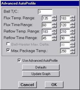
Protection of a thermally sensitive package with low thermal conductivity can be achieved by monitoring and limiting the temperature at the top of the package. By setting Figure 6 – Advanced Auto Profile Rules Screen a rule to limit the package temperature, the normal profile parameters are automatically modified to meet the constraints set by the rule (see figure 6).
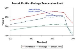
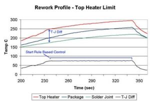
A profile was generated for the plastic BGA package (original profile shown in Figure 3) with a rule limiting the package top temperature to 250°C. A thermocouple was attached to the top surface using thermally conductive epoxy1. Careful attention was paid to avoid creating excessive surface area on the epoxy bead attaching the thermocouple. Typical parameters were used as a starting point for profile definition(6). The additional package top temperature rule was imposed.
The Auto Profile software functioned as normal until the temperature measured at the top of the package reached the specified limit. Once the limit was reached the top heater control switched over to Rule Based Control (see Figure 7). The ramp rate was automatically adjusted to maintain the temperature within the limits. Reflow dwell time was dynamically corrected to keep time above liquidus within the specified range (Reflow Time Range). The resultant package temperature exceeded the limit by two degrees, but remained 15 degrees lower than the profile that was generated without application of the rule.
Having the ability to monitor the temperature at the top of the package and automatically provide correction during the “Learn” phase of profile generation is a powerful tool in the task of protecting delicate components. If the two degree overshoot allowed by the algorithm exceeds acceptable profiling goals, an offset can be included in the rule (i.e., setting the limit to 248°C) to satisfy this requirement.
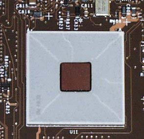
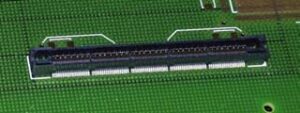
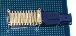
Many types of components may benefit from this approach (see Figures 8a, 8b and 8c). For instance, a popular Flip Chip BGA construction leaves the bare IC exposed directly to hot gas. The bodies of leaded surface mount connectors often have strict temperature limits (typically 160° C). The optical elements within fiber optic transducers and receivers quite often must be held well below reflow temperatures. In all of these cases the sensitive areas of the component may be instrumented, and rules set to maintain the profile within prescribed limits.
| Figure 8a – Flip Chip CBGA | Figure 8b – SMT Connector | Figure 8c – Optical Transducer |
 |
 |
 |
Alternative Approach
There are often circumstances when the attachment of a thermocouple to the top of the package is not convenient or perhaps not possible. For instance, it is not practical to permanently attach a thermocouple when a limited number of boards are to be reworked. In these cases a simple alternative rule may be applied.
Rather than having to measure the actual temperature at the top of the component, previously established data can be used to define the temperature relationship between the top heater and the top of the package. This relationship is based primarily on the materials and construction of the component.
A review of data from the prior rule based profile (Figure 7) shows that for the PBGA construction in question, a maximum package temperature of 250°C can be maintained by limiting the top heater to no greater than 70°C above the solder joint temperature during the reflow portion of the rework profile.
The new rule to limit the temperature difference between the top heater and the solder joint was specified. The thermocouple on the top of the package was left in place for data collection only – the feedback was not used to set the profile. The Auto Profile “Learn” sequence was again executed.
As the profile approached peak reflow temperature the top heater control maintained the specified solder joint ramp rates and temperatures. Several seconds after the solder joint passed liquidus, the temperature difference between the top heater and solder joint reached the maximum. At this point the top heater switched to Rule Based Control. The ramp rate was automatically modified. The reflow dwell time was dynamically adjusted to keep the profile within specified minimum and maximum time over liquidus.
The resultant profile is shown in Figure 9. The peak package top temperature was 253°C, nearly the same results as those achieved with control using feedback from the package top. Again, the desired protection of the component was achieved. However, obtaining consistent results requires knowledge of the package materials and construction, and experience with similar package types in order to determine the proper limits to apply.
Conclusion
Over the past five years great strides have been made in the development of software packages to assist in the generation of a thermal profile without having to resort to traditional trial and error methods. However, the profile has invariably been based on the need to subject the solder joints on a component to a given set of thermal process conditions. It has often not been possible to take into account the harmful effects that can be encountered by, for example, other parts of the same component that are particularly temperature sensitive.
This paper has highlighted the need to be able to control heat sources in such a way that the desired soldering requirements can be attained while, at the same time, avoiding damage to sensitive components. It has been shown that Rules Based Thermal Profiling goes a long way to achieving these objectives and, as a consequence, seemingly incompatible constraints can often be overcome.
Though not every set of constraints can be met by imposing rules – i.e., one can not ignore the laws of physics – many conditions can. Strategies for applying rules, and algorithms employed within the control software, will continue to evolve to meet new and more difficult requirements.
Rules Based Thermal Profiling offers the Process Engineer the ability to more easily tailor rework processes to satisfy today’s increasingly stringent needs and still maintain the yields and reliability that are paramount in the current market environment.
Acknowledgements: The authors would like to thank Bryan Pinette and Jeff Samuelson for their ingenuity and extensive effort in development of the software platform that enabled Advanced Auto Profile and Rules Based Profiles. We would also like to thank Ernie LaFleur for his insight into process requirements and system controls that proved invaluable in development of the algorithms on which the rules are based.
References:
1 Loctite 384, Thermally Conductive Epoxy, Henkel Loctite Corp, Rocky Hill, CT 06067.
2 Materials Engineering – Material Selector 1993, Penton Publishing, Cleveland, OH 44114.
3 Loctite 3142, Data Sheet – Potting and Encapsulating Epoxies, Polyurethanes, Hot Melts, & Silicones, Henkel Loctite Corp, Rocky Hill, CT 06067.
4 Application Note DC-004, DC/DC Converters, Beta-Dyne, Inc., 110 Elm St., Unit 12, Bridgewater, MA.
5 Jones, M & Jones S., Basic Mechanical and Thermal Properties of Silicon, Technical Publication of Virginia Semiconductor, Inc., 1501 Powhatan St., Fredricksburg, VA 22401.
6 Naugler, D., Thermal Process Development for Rework, Proceedings, Nepcon 2000, Anaheim CA.